
What Is Semiconductor Design?
Semiconductors are some of the most simple electronic components, but do some of the most complex tasks imaginable. They are manufactured from silicon, one of the most abundant elements in the earth’s crust. Molten silicon allows a chemical bond to grow a bell shaped parcel called a boule or ingot around a seed particle, creating uniformity, consistency, and traits that allow the silicon to be sliced microscopically thin or formed into tiny bodies that make up electrical components. Semiconductors are created when various elements, such as phosphorus containing soil, are added to the silicon, giving the final product different characteristics.

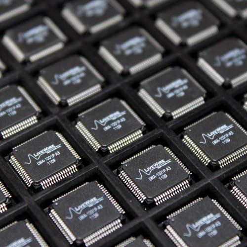
Semiconductor material is the core of integrated circuits, also known as monolithic integrated circuits, IC’s, microchips, or just plain chips. By combining a large amount of tiny transistors onto a chip, a very small chip can be designed that provides faster, more reliable components for electronic devices that are inexpensive to produce, durable, and use less energy and generate less heat. They can be mass-produced by semiconductor companies in generic configurations or specifically designed components. When semiconductors are designed, they generally fall into the category of digital or analog, depending on the need and cost point of the parts needing manufactured.
Semiconductor products can be mass-produced, allowing for large quantities to be available at a low cost to the market. They can be tailored to custom designed needs, and are often procured through a fabless design firm that engineers specific electronic components to meet the exact needs providing functions or exact tasks in a manufactured device. All manner of electronics from computers to mobile devices to appliances and medical equipment use semiconductors, and many of them are generic or have been designed specifically to meet the particular needs of a company’s final product. Their low cost and wide availability have made consumer and industrial electronic prices drop, making products more widely available to a bigger marketshare, and the small size has made increased computing power available in smaller and smaller packages.
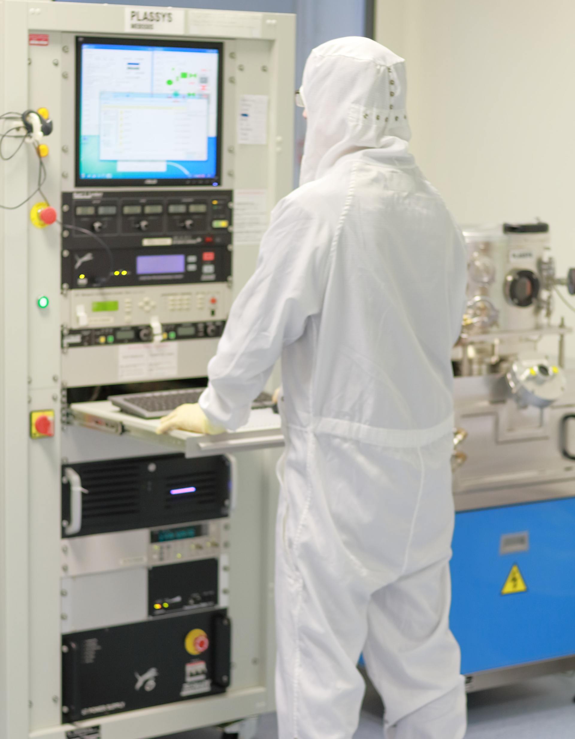
Since the 1970’s chip size has continued to decrease with improved materials and manufacturing standards, while increasing capacity. They have some distinct advantages in that they are lower in cost and better in performance than transistors or discrete circuit electrical components. They use little power, can be placed in proximity due to low heat bleed, and are often produced utilizing a process known as photolithography. This process uses light to transfer a pattern or “mask” to the surface of the silicon slice that is then treated with chemicals to etch the pattern into the surface. This photomask process, while expensive, allows good commercial viability in production, as the design work can be done in a fabless design company such as US-ASIC by one of our highly qualified ASIC engineers, then outsourced for manufacture.
Ranked as one of the top fabless semiconductor companies 2015 and several other years, US-ASIC welcomes the opportunity to solve your component needs. Contact us and one of our highly experienced ASIC design engineer staff will personally work with your research and development team to learn what you need and how we can design components to make your products and equipment more efficient, cost effective, and ease the burden of manufacturing those components for your company.
What is Fabless Semiconductor?
A fabless semiconductor might be easiest understood as a generic product. Fabless semiconductor companies like US-ASIC design hardware components such as silicon semiconductor chips, wafers, or other components, and then have them manufactured elsewhere at a manufacturing plant that specializes in components. These foundries may make just one type of component, or a wide range depending on their tooling and equipment. The advantage of specialized manufacturing allows maximum utilization of research and development resources, resulting in a final product at a lower cost. It also allows for exacting inspection and quality control, providing an end product of high quality at a good price. Often this means a supplier can provide very competitive pricing on inventory custom designed for a client, such as a fabless semiconductor supplier specializing in analog components. By utilizing a fabless component company, companies can leverage their R & D budgets as well as material expense while being able to get specialized semiconductor chip design and production runs at a far better price point. This solution works well for both small batch and large volume production runs.
Using centralized manufacturing at a facility specializing in components, quality and cost control are tantamount. In the old days the component industry was nearly all vertically integrated. Companies that made semiconductors built their own manufacturing plants, did their own research and development, secured their own materials, and tooled independently. This meant they also did their own stamping and assessment for quality standards. This created a marketplace with very high cost of entry barriers, making it extremely difficult for small companies to get a foot in the door. As the availability of manufacturers of integrated devices arrived at increased capacity and efficiency, they found they had capacity to produce more than their own needs, leading to opportunities for smaller companies to have their components manufactured through outsourcing, saving expense, time, and assuring quality control. This led to the opening up of fabless semiconductor business model where companies could handle the design engineering for custom work or standard procurement for clients without the expense and issues of owning their own factory.
This focus allowed specialization in semiconductor chip design, as well as other components, by fabless companies, allowing their clients to have guaranteed sources of the parts they needed that could also be specialized to their needs, improving their final assembled products. This supply chain dynamic streamlined the availability of silicon components while bringing the cost down, allowing tremendous development of new products for industry and consumers.
A Little History About Chips and Chipset
Many people think the advent of silicon wafers and chips is a relatively new invention in the field of engineering, but it actually has a long history of development. The first discovery of a semiconductor diode, a device that has two terminals that generally allows current to flow in only one direction, was in 1847 by Karl Braun, a German physicist and inventor who contributed heavily to the development of early radio and television. Braun observed that current would flow freely in only one direction between a metal contact and a galena crystal. His work led to the first semiconductor patented in 1901, called a “cat whiskers”. He received a Nobel Prize in Physics in 1909, which he shared with Marconi for work in the development of “wireless telegraphy”.
Much of Braun’s work was set aside and forgotten about until World War II and the need for radio and telegraphy controlled equipment. Work throughout the war era led to the first computer built by the University of Pennsylvania in 1946, consisting of a building full of vacuum tubes. Realizing the need for a more efficient component system, Bell Labs developing the point transistor in 1947, and further research grew exponentially until the integrated circuit was developed in 1959 by Kilby at Texas Instruments. Semiconductor design engineering at first was focused on calculators for business application, helping to speed the time it took to keep books, post ledgers, write payroll, and tally inventory. Semiconductors, integrated circuits, and a myriad of other components now touch and are integral in nearly every part of our lives, from household computerized speaker systems we talk to, to hand held fully functional computers with voice and visual capacity called cell phones.
While silicon is still the most widely used material in semiconductor manufacturing due to its inexpensive raw material costs, availability, ease of processing, and applicable temperature range, there are other materials that are now being used extensively in manufacturing. Germanium, in particular, while thermally sensitive, makes for an excellent silicon alloy for high-speed devices. Other materials include gallium arsenide, silicon carbide (often the material used in blue light emitting diodes or LEDs), various indium and selenium compounds, and some organic compounds. Research continues at semiconductor design companies to locate materials that are cost effective, provide improved or new conduction results, and can be manufactured effectively in substantial enough sizes with sufficient temperature ranges for chipset design applications throughout a number of different industries.
Today’s manufacturing and even specialized company needs require the ability to design, engineer, and manufacture specialized semiconductor and other components to push today’s mobile, computer driven economy and society. Having a team that can do the specialized semiconductor design engineering for your company, as well as source and supply the final components at a highly competitive price with outstanding quality control, gives your company the cutting edge it needs to be competitive and to stand out in your industry.
Why is Chip Design so crucial?
Until the advent of semiconductor devices, most equipment that required electrical current to be conducted to create a result, or finite response, required vacuum tubes. Tubes were made of ceramic, metal, or most often borosilicate glass and fine metal filaments consisting of an anode and a cathode with a heater, often tungsten, and controlled electrical current under a high vacuum pressure, often in a suspended gas. Early thermionic tubes were able to handle signal amplification and current rectification, as well as other effects. Non-thermionic tubes or “valves” provided photoelectric effects that could sense light levels. The development of anode tubes was responsible for the development of radio, television, radar, sound recording and reproduction, the ability to design and implement long distance telephone networks, as well as both early analogue and digital computing devices. Vacuum tubes were expensive to produce, bulky, fragile, temperamental, and gave off tremendous amounts of heat.
The advent of the first solid state devices in the 1940’s, semiconductors, provided an alternative to vacuum tubes that were vastly smaller, gave off little heat, much cheaper to produce, easier to transport, and were far more durable and reliable. Semiconductors also need a low voltage supply to operate, far lower than a vacuum tube, making their operation much more economical. Their shock-proof capacity and small size allowed their use in many more applications and led to digital computers moving from an entire building or room to something you can hold in your hand at a far more economical cost. It also allowed detailed, specific engineering by firms such as US-ASIC to provide top quality analogue integrated circuit design, digital integrated circuit design, and other semiconductor design engineering through fabless semiconductor implementation that is cost effective and highly efficient to produce components that do exactly what you need done at a fraction of the research and design cost, as well in house manufacturing expense, to meet your company needs.
What is a Chipset?
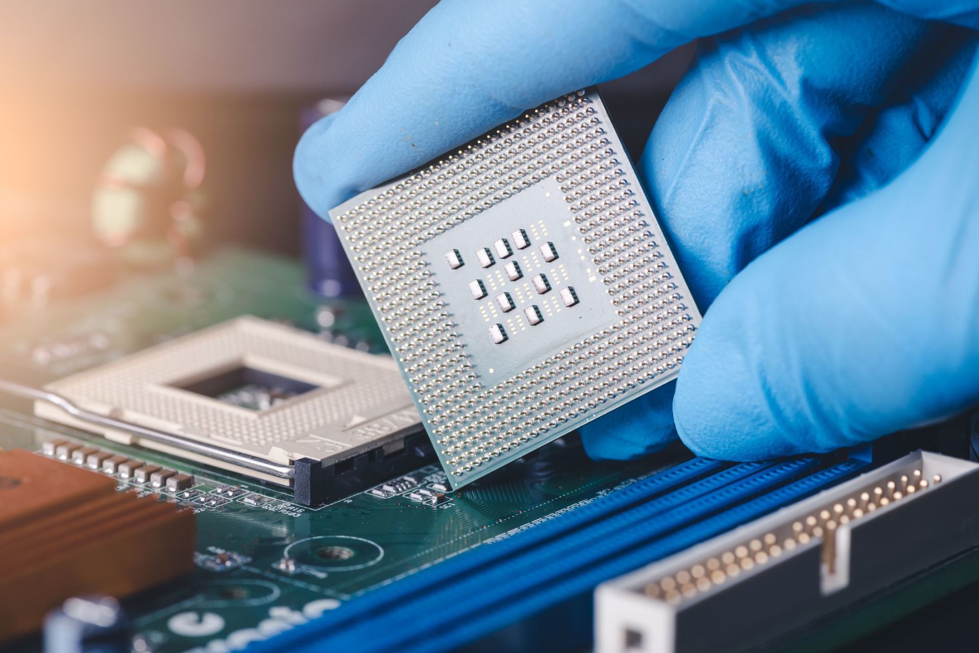
To explain what a chipset is in ordinary terms, you can think of it as the “gatekeeper” or central hub in an integrated circuit in a computer system. The term used for a chipset is a data flow management system, because it regulates the data as it passes between the processor, the memory, and the peripherals (things like printers, monitors) in a computer system. A chipset is actually a group of chips or integrated circuits that work between the central processing unit, or CPU, and the devices, ranging from buses, memory, and sometimes printers or monitors or other external peripherals. It is usually on the main board, known as the motherboard, in a computer, and is core to the electronic, and therefore data, traffic that passes through and to the various parts of that computer. Chipsets generally are specifically designed to work with certain types of processors and devices, speaking their individual “languages”. The chipset is what not only processes, but helps translate that language, significantly aiding the computer’s performance and ability to process and do the job assigned correctly and quickly.
It is important in processor design to make certain that chipsets and CPUs are chosen that work together and are complementary in function and flow. Chipsets are manufactured to work with specific CPUs, and since they are integrated into the main motherboard of a system, they cannot be changed, upgraded, or removed. This means that hardware configuration and design is important so the sockets all fit and match, and that the working flow optimized for both the chipset and CPU so the system runs efficiently and accurately. Our fabless semiconductor and processing design staff at US-ASIC knows how to match chipsets to CPUs, maximizing what the components can support and the best fit for your applications. This is especially important in graphic design applications where cost of the video cards is especially important to have the best flow, response time, and quality available in a final product while controlling production expense.
Another important application is for artificial intelligence applications. AI is increasingly important in many industries as a means to control production costs, act predictively for line adjustments, FIFO and other materials control, and to optimize performance of equipment. Correct design utilizing chipsets, CPU, and other components can provide the best computing ability while maximizing energy and other resources in AI applications. Our integrated circuit design engineer staff can solve your AI challenges, and provide chipset compatibility at a good cost that meets both your budget and AI integration needs. We are on the cutting edge of deep learning chipset design and our fabless structure allows us to utilize manufacturers that can meet your demands quickly and accurately whether you need a simple, minimal dedicated function chipset, or a more complicated embedded chipset that is able to handle a variety of different tasks and programming functions.
What is Digital Signal Processing or DSP?
Digital signal processing, or DSP as it is commonly called, uses digital signals in the form of a string or series of numbers that stand in for a common or like variable in something a semiconductor design engineer is trying to quantify and represent, such as a frequency (wavelength), time, or distance/space. The digital signal appears as a continuous pulse, which is valuable in digital signal processing. DSP is commonly used when signals involving audio transmission are involved, such as speech transmission on cell phones, voice recognition, RADAR and SONAR applications, some types of financial reports, and seismic activity for the detection of earthquakes and tectonic plate shifts. In application, DSP also can digitize pressure and images, the later being used for medical diagnostic tools. DSP converts a signal from analogue to digital utilizing a mathematical formula that has been programmed to recognize the patterns and process them, based on how the processing equipment is constructed.
DSP has some big advantages in semiconductor design as signals obtained from a digital source are far less affected by noise, distortion, or forms of interference. They are easier to design and cheaper to produce than analogue circuits, and the work to configure them to custom application is generally easier and cheaper. DSP works for both streaming and stored (static) data equally well. They provide a higher degree of accuracy, and by nature can be configured into much more complex applications in custom designed systems. Large amounts of digital data can be stored inexpensively and compactly via magnetic tape and other methods with no loss of reproductive quality over time, making DSP ideal for large and sensitive data storage for industries requiring medical or financial security and privacy compliance. There are also advantages in detection of errors and methods to correct errors within data computation and processing using DSP over analogue.
This is why fabless semiconductor companies list many specialized applications that their design staff can create specialized components towards that utilize DSP, streamlining design and manufacturing specific to a company’s individual processing needs. At US-ASIC, our fabless semiconductor design staff can create DSP processing engineering for your applications that maximize potential and integrity of data while minimizing component cost and processing issues. Many DSP processing events can be run on standard computer equipment or designed into application specific integrated circuit (ASIC), microprocessor design, field programmable gate arrays (FPGA), industrial applications for controller devices, and various stream and signal processing systems. They are often a very economical option that provides a mathematical solution to many real-time and non-real time processing needs.
What is FPGA?
The advent of increasingly complex component systems required for capacity, AI, and development in general have brought field-programmable gate array or FPGA integrated circuits to the forefront in semiconductor design in recent years. A FPGA is a silicon chip or circuit that allows configuration or programming in the field or post manufacture. The unit can be initially programmed during manufacture or left “clean”, but the ability to easily reprogram or tweak the functions of the component in actual live-time application allows for calibration, changes, adjustments, or full reprogramming to another purpose without having to dismantle or replace an entire system to achieve the new desired result. FPGA contain a multitude of configurable logic blocks and programmable interconnection circuits that allow them to be utilized in a variety of applications where complex logic functions are needed. They are not designed in advance to do specific tasks, meaning they can be manufactured faster. They are extremely flexible in application, and can be reused many times. Their design allows a large amount of data to be able to be processed through them, and they have found application in a wide variety of industries ranging from defense and aerospace to financial, data, performance, medical, security, video and image processing, and other uses.
A significant advantage for FPGA application is they are far less expensive to develop than an ASIC system. Their function capacity and flexibility, however, means they can stand in while development and testing is being done on a new device until all the adjustments are complete, then an analogue integrated circuit design can be developed usually faster at less expense from the prototype work. This makes FPGA to ASIC conversion a financially attractive alternative in fabless design and development, providing expeditious results at a lower price point for overall manufacture of complex electronic designs. Prototypes can be reprogrammed by an on-site coding editor, making adjustments fast and accurate. Since the generally proprietary software or “firmware” is updated in circuit, the FPGA functionality stays current. Since most final ASIC chip is expensive to design, develop, and manufacture, the ability to have all testing and adjustments done in “real time” provides complete, complex, complicated results that have undergone rigorous testing, assuring the final product is correct and as close to flawless as possible. With much equipment now being designed around software, the ability to utilize hardware that guarantees a fluid testing process that integrates into the software puts FPGA at the cutting edge for cost effective, practical research and development and manufacturing systems.
It is important that any system utilizing FPGA start with a design team well versed in digital logic design, as well as FPGA coding. FPGA coding is far different than other coding applications, and is based on HDL and VHDL (roughly based on C and Ada). A full service fabless design team with expertise in both ASIC and FPGA function and interrelation can provide seamless development of components to meet the applications critical to the success of your electronic needs. If your design has potential for adjustments, modifications, tweaks, upgrades, or needs on-the-fly programmability, an FPGA may be a wise place to start your development stream.
What is ASIC?
When you are in need of a microchip that is designed and manufactured for a specific need, task, or application, such as running a crypto-currency miner, quality digital recording equipment, or finite sized component applications such as in hand held devices, an application specific integrated circuit or ASIC may be the best component for your needs. At US-ASIC we specialize in high-tech design of ASIC components that will do exactly what you need done, when you need it done, at lightning speed. ASIC chips are energy efficient and can handle code effectively and cheaply, and you can expect precise results every time. Multiple units made for execution can be integrated on a single board, increasing speed and performance. While often costly to develop, when you need accurate performance with no margin for error, an ASIC component is well worth investigating.
Many ASIC components rely on good digital signal processing, or DSP, to clean up, clarify, or standardize the data signal for specialized or particular usage. That DSP-ASIC engineering design requires knowledge of advanced component integration, and our engineering staff at US-ASIC specializes in high level, complex component systems utilizing DSP interface ASIC applications. ASIC can be expensive to develop, and in some applications, time consuming or requiring a sizeable outlay of resources due to the nature of their function. That is why our team often recommends DSP-FPGA-ASIC staged development or bread-boarding, followed by testing, and implementation so all parts of a system can be designed, prototyped, tested repeatedly, finessed, and only when exact and your application is met, a final design is sent for manufacture at a fab house. This allows a final production run in large quantities with few issues, making the per unit final cost significantly reduced.
Thanks to the extensive research and development of new materials and manufacturing processes, ASIC have moved from being able to house about 5,000 logic gates to over one million. This has increased the maximum functionality of them as well as made them able to handle much more complex operations. They can be combined within a total system design including but not limited to integration with ROM, RAM, microprocessors, and other components during a design and build. Available in manufactured form as gate-array designs (pre-manufactured and ready to assemble) or fully customizable, there is a wide range of design nuances that can allow an ASIC to perform tasks as independent or integrated as your needs require. Their small size, low energy requirements, and high performance capacity can provide your company a competitive edge with flexible design options that solve a myriad of tasks in a compact component. Another advantage of ASIC design is the ability to provide intellectual property protection within the design, creating a protected, proprietary component that gives your design and product an edge in the marketplace. Contact US-ASIC and you can be assured of a fully transparent, integrated team approach to designing, testing, and implementing an ASIC component creation that works for you.
Check out some of our solutions here:


Northern Europe/Scandinavia
Contact: Lars NilssonTel: +468 6695650E-mail: Lars.nilsson@us-asic.com Mobile: +46 70 5958081
Asia
Contact: Steve ChoiTel: 82-2-2057-2877
(#1000)E-mail: asifs@norcalts.com
Privacy Policy | Terms & Conditions | Copyright 2022 U.S. ASIC | Website & SEO by Iron Oak Marketing